IPM-UNFC
Universal NandFlash Controller
Overview
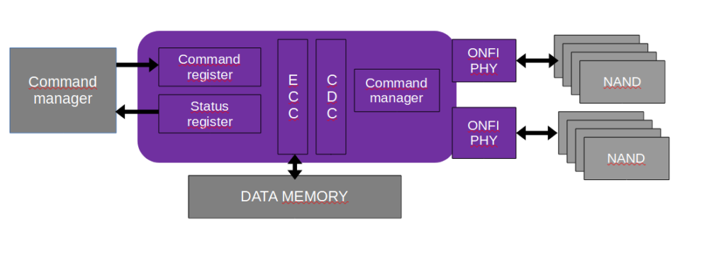
IP-Maker’s Universal NAND Flash Controller (IPM-UNFC) IP core is designed specifically to enable commodity Flash memory to be effectively used in enterprise storage applications requiring high reliability and large interconnect bandwidth. Using the pre-validated IPM-UNFC IP allows greatly reduced time-to-market for storage OEMs desiring higher IOPS benefitting from lower cost SLC, MLC , TLC & QLC NandFlash memory.
The IP-Maker IPM-UNFC is full-featured, easy to use in FPGA and SoC designs. For ease of integration with the system interfaces, three native backends (AXI, Avalon and RAM) are provided. The IP core allows page size configuration, spare size per channel.
- ONFI 5.X Compliant
- SLC / MLC / TLC / QLC
- SDR modes 0 to 5
- NVDDR modes 0 to 5
- NVDDR-2 modes 0 to 8
-
NVDDR-3 modes 0 to 10
- NV-LPDDR4 modes 0 to 15
- AXI or Avalon interface
- Optional DMA interface

ECC
- Configurable BCH to NAND's vendor requirements
- configurable matrix to follow the NAND's requirement BER
NandFlash interface
The NAND flash interface handles all the hardware compliant process (command, address and data sequences). It is ONFI 5.x compliant. Data and Metadata can be protected by the ECC by using configurable data block size (e.g. 1024 bytes + x metadata bytes.)


