
The internet of everything, from small sensor to autonomous car, is driving a huge data deluge from embedded systems. These data provide high value for the end user or for the service provider. This value is generated from the data thanks to analytics computing. Typically, it is done in a cloud environment. In a near future, the amount of data will be so huge, therefore part of the storage and analytics must take place in the embedded system itself to avoid the saturation of global network and cloud infrastructure.
Even if the data are stored in an embedded system, it requires the same level of security as a cloud environment, or even higher since a physical access can be operated, which is quite impossible for the data stored in a cloud data center.
This security protection can be achieved with the use of an encryption engine that uses a local key. Let’s see how to store and protect this key.
The challenge here is to provide a high security level, within embedded constraints such as limited storage capacity, reduced computing capabilities, small space and a limited cost and power. Typical embedded systems are running their application on a system on-chip (SoC), with interfaces such as USB, SATA and Ethernet. These systems are quite easy to design since the overall ecosystem is wide, with many solutions for embedded software, real-time operating systems and drivers. On the storage side, the encryption key could be stored in an attached USB drive, but this is not secure enough as it can be removed easily.
A more secure design is required. That can be done with a custom design, based on a FPGA, connected to the SoC through a PCIe interface. The PCIe interface is powerful, with a low latency and a high bandwidth. The drawback is the development cost. FPGA provide the best performance/ratio, but that requires very strong skills for the R&D team. Instead of designing everything on the FPGA, their value is on the full system design, and not on the interface. Then, an off-the-shelf PCIe interface may be useful in order to reduce the design and validation time.
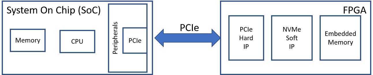
Embedded system architecture: Soc and FPGA-based secure NVMe Drive
IP-Maker provides a full hardware NVMe IP. It is based on an automatic command processing and a multi-channel DMA. It can be easily implemented in a FPGA, as a bridge between a PCIe interface and a DRAM. It is an ideal solution to implement a standard data transfer mechanism, providing low latency and high bandwidth. It comes with standard interfaces, such as Avalon and AXI bus interfaces. A NVMe IP for FPGA can be used for high performance SSD, write cache card, computing accelerator or even for a NIC. In our example, it is used as a secure embedded drive.
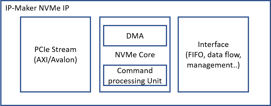
IP-Maker tiny NVMe IP
Let’s analyze a full embed system, based on a host and its attached drive. The host (a SoC), can run a standard NVMe driver in a Linux environment. At power up, it will automatically detect and configure the FPGA-based NVMe device, which is connected to the PCIe interface of the host. Then the host see a storage space: this data space can be used as a storage area. The NVMe IP from IP-Maker successfully passed the NVM Express certification. Demonstration are available on a wide choice of FPGA evaluation kit from both Intel and Xilinx. Performance benchmark can be easily done with standard tools such as FIO or IOmeter.
In a data center environment, with a PCIe Gen3x4 configuration, this IP is able to reach 3.2GB/s of data transfer, more than 750kIOPS en3x4, and about 10 µs latency.
In an embedded system environment, as a secure drive, the performances requirement may be lower, a PCIe Gen 2 interface with 1 lane, may be sufficient. The IP-Maker NVMe IP is fully configurable at the design stage. It is based on a modular approach, then most of the advanced features and performance accelerators used for the data center applications may be removed. That leads to a tiny NVMe IP with a very low gate count, which is perfect for small embedded FPGAs, which is compatible with the embedded constraints in term of cost and power.
In a full FPGA design, this NVMe technology will be integrated between the PCIe and the DRAM buffer. A CPU, SW or HW, will be embedded as the orchestrator. IRQ lines from the NVMe user interfaces will help the CPU to manage NVMe transfer. And finally a specific hardware for the computing algorithm accelerator. When the host CPU wants to process some data with the FPGA accelerator, then it sends these data to the NVMe driver. The NVMe IP will manage the data transfer from the device side and store it in the DRAM buffer.
This FPGA NVMe-based solution is perfect to store encryption key in an embedded system. That allow the use of a standard SoC coupled to a FPGA, without requiring a power-hungry and expensive high-end CPU.
That solution delivers a best-in-class security protection with the design constraints of an embedded system. This NVMe IP coming with all the design environment will allow your team to focus on high value hardware development, therefore reducing the total development cost.
This configurable NVMe IP based on a modular architecture can be used in various embedded systems, from a secure drive to high performance embedded storage. That will be easy to select the right design options in order to reach the technical specifications in term of performance (bandwidth and latency), NVMe features, and gate count.
As NVMe is becoming a standard interface for high performance data transfer, that’s a good time to start designing with it. Thanks to its full hardware architecture, it is already powerful enough to be used with storage class memory, such as MRAM or ReRAM. Then for next gen FPGA-based system that requires SCM for a local NVM buffer, the NVMe IP from IP-Maker is already set. Start design now, and make this NVMe-based architecture the platform for your next generation of powerful embedded systems.